


The next great challenge for storage companies will be developing a Storage Class Memory (SCM), a nonvolatile memory with access speeds, granularity and other characteristics more like DRAM than flash. However, the enormous promise of SCM in computing environments cannot be fulfilled unless the technology can escape the challenges of scaling.
How can such a potentially fast, powerful, and high capacity technology be developed in a way that is both practical and economical enough for widespread commercialization? One approach is to draw on the lessons learned in developing 3D NAND.
The Necessary 3D NAND Revolution
2D NAND, the work horse of the solid state storage industry, had scaled effectively for almost 10 generations until the music stopped. The fact is that the cost of fine pattern lithography, the number of electrons that could be stored in the floating gate and the disturb effects from cell proximity made further scaling impossible. The economics and physics of shrinking 2D NAND below 15nm and scaling devices horizontally on a single plane simply do not make sense. The 3D NAND revolution had to happen, and since it’s happened, the pace of adoption has been breathtaking.
The concept itself of stacking memory cells vertically, meaning allowing high cell density while side-stepping many of the scaling issues, is not new. However, developing it took time. Yet even more importantly, this technology revolution could only happen once we hit the right price point to embed it into products that we can actually bring to market. Until we could do that, it would simply remain an interesting architectural discussion.
So how did we transform this into a scalable technology, and what does it take to bring cost down in order to bring products to market at a competitive price point? The answer is scale. Massive scale.
Massive, Massive Scale
When discussing scale at mammoth proportions, it’s often easier to use a graphic visualization to make a concept easier to grasp. Imagine we would stack a tower made of NAND wafers produced in 2016 in our joint venture fab in Yokkaichi alone – how high would it reach?
Keep in mind that the thickness of a standard silicon wafer is about half a millimeter, which is very, very thin to say the least. So how high would this stack be? As high as the Empire State Building? The Eiffel Tower? The world’s tallest skyscraper, Burj Khalifa?
If we look at the total number of 2D and 3D NAND wafers that will be produced in 2016 in the fabs in Yokkaichi, Japan (a joint venture with Toshiba) alone, this stack would be as high as Mount Kilimanjaro, Africa’s highest mountain, soaring at 19,340ft.
Now that’s MASSIVE scale!

Moving Mountains of Data: Storage Class Memory
With this concept of vertical architecture and scale in mind, let’s move on to what I really wanted to talk about – Storage Class Memory.
I’ve been in this industry for the past four decades and have witnessed the progression of computer technology first hand. DRAM and SRAM technologies have been here since the 1960s, and they are still broadly used today. Certainly, the technology has advanced and capacities have become greater, but we are still talking about the same underlying technology. And they are still very expensive.
If we look at the spectrum of storage devices today, there is a huge performance gap between DRAM and primary storage devices like HDDs, and even SSDs. This is the challenge ahead – filling this gap with a technology called Storage Class Memory (SCM). Positioned between DRAM and primary storage, from both a performance and a price point perspective, SCM is nonvolatile memory with access rates, endurance levels and other characteristics far more like DRAM than flash.
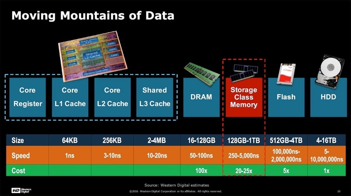
You can clearly see why the promise of Storage Class Memory is revolutionary for the industry as a whole. But the promise cannot be fulfilled unless the technology will be able to tackle the challenges of scale – both practical and economical.
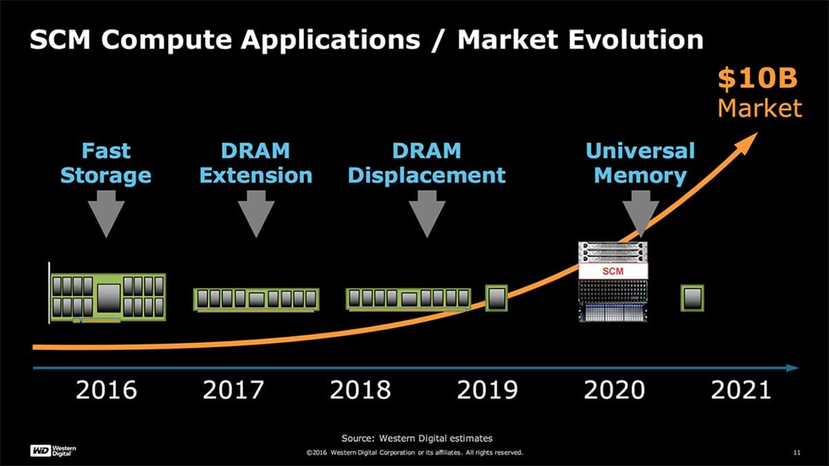
The approach I’d like to draw from is the lessons we’ve learned in developing 3D NAND. Sure, the technologies differ, but memory engineers still have to tackle the issues of cost, scalability, performance and scale, just like our engineers did for 3D NAND. It took almost a decade from the original concept of 3D NAND to high volume market acceptance.
The Future of Storage is Bright, and Scalable
The evolution of storage is, and will be, one of the major drivers in the industry. Our success requires not only having a storage portfolio that is the largest in the industry, but also being among the most innovative ones.
The recent launch of our next generation 3D NAND technology called BiCS3, the world’s first 64 layer 3D NAND, features the use of 3-bits-per-cell technology along with advances in high aspect ratio semiconductor processing to deliver the smallest 256GB chip in the industry to date and densities up to half a terabit on a single chip.
This technology is already being implemented in USB devices and SSDs, is being sampled by OEMs today and will likely spread to wherever possible for flash to go into. It’s happening not just because we could overcome architectural challenges, but because we could hit the right price point for the customer. Until that happened, the technology remained a demonstration vehicle, not a viable, scalable technology.
This is the challenge ahead for Storage Class Memory. Memory engineers must follow similar approaches to the lessons learned from 3D NAND if they are to unleash its enormous promise.
Watch the unveiling of 64 layer 3D NAND model and excerpts of my keynote at Flash Memory Summit 2016 below: